RTL Circuit Design for Boolean Expression Realization
Transistor-level implementation of Boolean logic gates.
Technical Deep Dive 🛠️
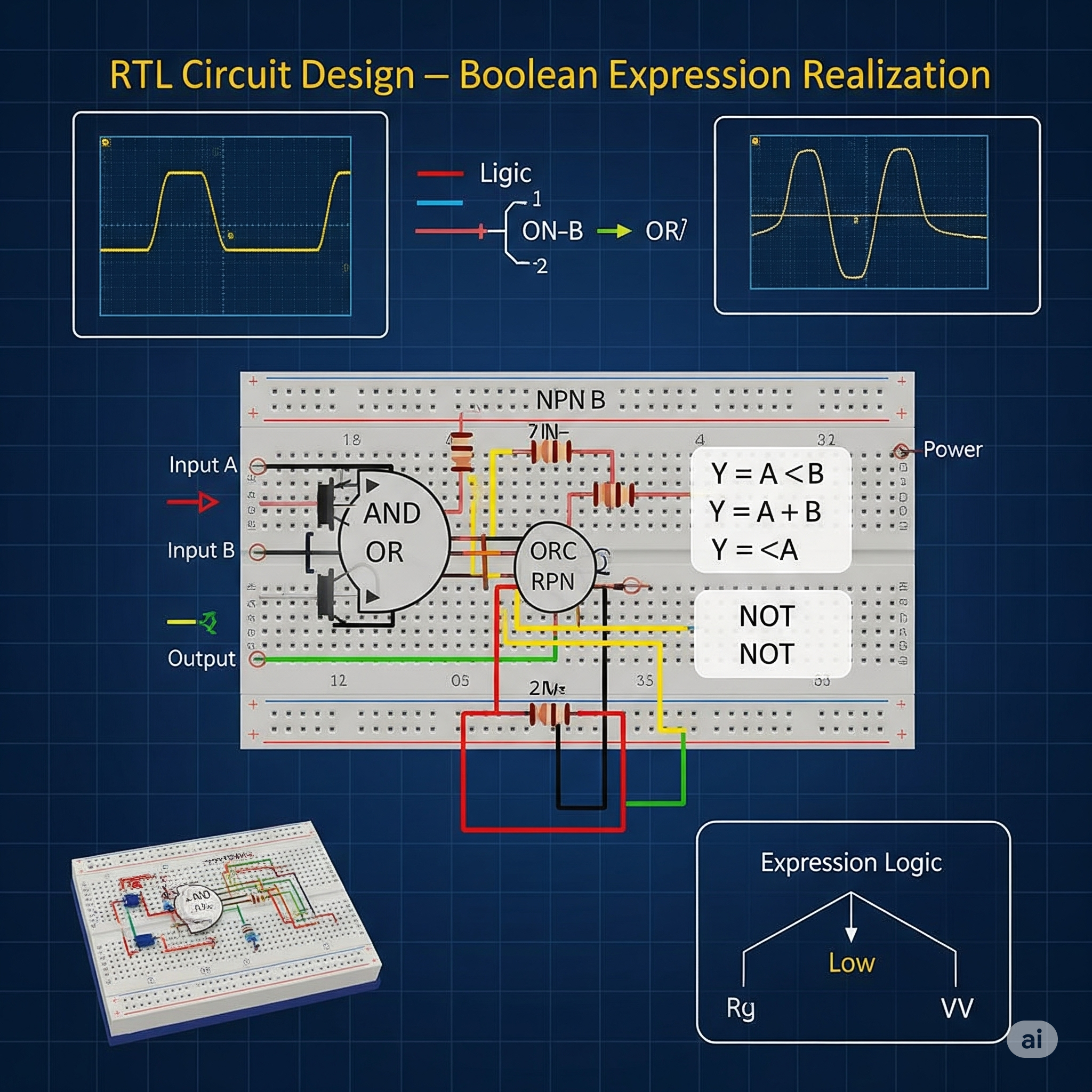
This hands-on electronics project involved the physical implementation of digital logic gates at the transistor level, providing deep understanding of fundamental digital circuits. Implemented Gates: • NAND/NOR universal gates • AND/OR with diode-transistor logic • NOT gate with single transistor • XOR with hybrid approach Design Characteristics: • 5V TTL-compatible • Fan-out of 3 • Propagation delay <50ns • Power <10mW/gate Practical Applications: • Educational demonstration • Custom logic prototyping • Understanding IC internals • Radiation-hardened logic basics Measurement Results: • Voh = 4.8V, Vol = 0.2V • Noise margin: 1.2V • Rise/fall time: 20ns
Engineering Challenges 🎯
- Noise immunity
- Fan-out limitations
- Power consumption
- Signal integrity
Achievements & Outcomes 🚀
- Working prototype on breadboard
- Used in lab demonstrations
- Foundation for ASIC study
- Research on variations
Technology Stack ⚡
Key Innovations ✨
- Transistor-level implementation
- All basic gates realized
- 5V TTL compatible
- <50ns propagation delay
- Educational focus